Introduction

We are an engineering services company in semiconductor & embedded domain. We work with our clients as an integrated team - from concept to completion. This high degree of interaction between our design team ensures that every little detail gets the close attention it deserves. Our work engagement models are quite flexible to suit customer needs.

Vision & Mission

  • Add value to our esteemed customer’s requirement without any compromise and become preferred partners in all our present and future offerings.
  • To deliver outstanding client service, to provide fulfilling careers and professional satisfaction to our people.

Who are we?

Green Semiconductor Pvt. Ltd. is incorporated by a team of talented and experienced professionals in the field of Electronics design, validation and testing. The promoters of Green Semi are having a combined experience of over 60 years in the areas of VLSI, Embedded design, Automotive and Test & Measurement equipment .


Design Services

RF and Analog Mixed Signal High Speed Design and Layout

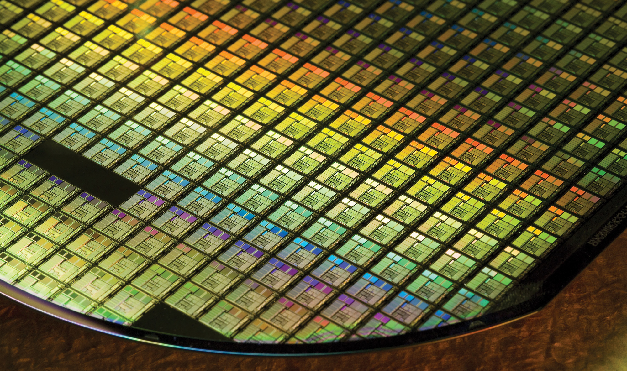
Green Semiconductors RF/Analog & Mixed Signal (AMS) team has silicon proven capabilities to handle Full chip RF IC Design, Layout including IO ring construction, ESD Protection, Full Chip Noise Isolation Strategy, Bonding diagram & Tape-out procedure.

  • RF Design, Layout & Verification
  • RF Path cells like SWITCH, LNA, RX MIXER, TX MIXER, POWER AMP & PLL
  • BASE BAND path cells like TX/RX FILTERS, ADC & DAC, XTAL OSC

Analog Mixed Signal and High Speed Design, Layout and Verification

Our Semiconductors Analog Mixed Signal (AMS) team has the capabilities to handle complex AMS Design & Layout. The AMS Team Expertise in

  • Analog Mixed Signal Design, layout, verification SERDES, High speed link design and layout
  • DPHY, MPHY, USB2, HDMI
  • Power management and STD cell
  • Experience in Silicon proven High speed phy layout and Silicon characterization with the latest node from 10nm FF to all upper nodes

Data Converter Design

We have capabilities to handle Complex data converter design:

  • 12 Bit SAR ADC
  • 18 Bit Sigma Delta ADC 10 Bit Sigma Delta ADC 8, 9 and 10 Bit SAR ADC
  • 10 Bit Pipeline ADC
  • Expertise from 4 nm Finfet to upper nodes
  • Test chip and IP delivery expert

Memory layout design and Verification

Our Memory team has good capabilities in

  • SRAM Layout Design DRAM Layout Design
  • CAM Layout Design
  • Compiler based memory layout design and full custom memories
  • Expertise from 7nm FINFET to all upper nodes Test Chip and IP Delivery Expert

Verification

  • VERIFICATION OF COMPLEX SOCS/ASICS FORMAL VERIFICATION
  • ASSRTION BASED VERIFICATION IP VERIFICATION
  • ARM / PROCESSOR & OTHER SUBSYSTEM LEVEL STANDALONE VERIFICATION
  • FUNCTIONAL & CODE COVERAGE CONSTRAINED RANDOM VERIFICATION POWER AWARE VERIFICATION

Business Model

Time and Material (T&M) Design Services

  • Green Semiconductors Provides Resources According To Customer need
  • Engineers work at customer site or In house
  • Task are supervised by customer and Green Semiconductors
  • Addresses the short-term resources requirements

Fixed Price Project

  • For a predefined scope and activity estimate with a defined start point and deliverable
  • Scope of turnkey engagement can be spread over different phases of the design service or solutions
  • Cost of the project is mutually decided up-front and the promised deliverables are executed

On-site ODC Services

  • Green Semiconductors builds dedicated team and operates as an exclusive design center for customer Projects at customer site
  • Team dedicated 100% to customer at customer site
  • Suitable for long-term dedicated resource requirements

In-house ODC Services

  • Green Semiconductors builds dedicated team and operates as an exclusive design center for customer Projects at our Site
  • Team dedicated 100% to customer
  • Suitable for long-term dedicated resource requirements
  • Isolated and secured network per customer at Green Semiconductors Site

Careers

We are hiring RF & Analog layout Engineers
  1. Experienced with RF layouts such as SWITCH, LNA, RX, TX, MIXER
  2. Layout Design of Analog circuits such as Op-Amps, Regulators, ADC, DAC, Power Management ICs, PLL.etc
  3. Standard cell ,IO cell, Memory Layout Design
  4. Tapeout Experience of Medium to Large Complex Analog Designs is an advantage
  5. Experienced with Linux/Solaris environment
Required Skills:
  1. Deep knowledge of Analog/Mixed signal physical design needs & techniques.
  2. VLSI layout design using CADENCE Virtuoso/Virtuoso XL
  3. Physical Verification Tools: Assura, PVS or Caliber tools experience is a must.
  4. Programming with SKILL/PERL/SHELL for enhancing layout productivity.
  5. CMOS Circuit Design knowledge would be advantageous.
Fill the form below, along with your resume and we'll get back to you in no time!
APPLY HERE

Contact Us

Registered Office

#150, 3rd Floor, 2nd Main
Kasturinagar (East of NGEF)
Bangalore - 560 043

No 37, 1st Floor,
11th Cross,
Belandur - 560 103


Contact Information

Email: info@greensemis.com
Phone: +91 90087 22799,
+91 99000 65971

Location Map

keyboard_arrow_up